


- Introduction
- Research Areas
- People
- Projects
- Services
- Facilities
- Achievements
- Gallery
- Contact
The Micro-Nano Manufacturing (MNM) group takes up projects sponsored by Indian Industries, Industry consortiums and Government funded R&D and fabrication of high-precision miniaturized micro and nano components having feature sizes in the order of less than one millimeter.
The micromachining facility at CMTI with its state-of-the-art infrastructure and expertise promotes the benefit of micromachining and ultra-precision technology for the manufacture of micro-components to the Indian industries through consultancy, services and training. The Micro-Nano Manufacturing (MNM) group focuses particularly on the development of product indigenization and fabrication services of high-precision parts.
The group is also involved in R & D and provides service in the area of nanofilms and nanocomposites by using state-of-the-art facilities like PVD and PECVD systems.
Using its experienced staff and dedicated state-of-the-art Femtosecond and Excimer laser micromachining systems, offers a completely flexible, leading-edge laser processing service by high precision, micro and nano-machining of components made of metals, glass materials, polymers, semiconductors etc.
Objectives of MNM group:
To offer micro-nano machining services to industries
Develop indigenous machining technology for Micro parts machining
Research and Development to achieve excellence in micro-nano manufacturing
technology
Human Resource development in the field of micro & nano machining
Development of machining technology for import substitution components of various
sectors/industries like automobile, aerospace, biomedical, defence etc.
- Precision manufacturing and micro machining.
- Indigenous Machining Technology development for newer materials and difficult to cut materials (super alloys)
Surface Engineering
- CNT, CNT-Metal/ Ceramic 2D Nano material
- Diamond Like Carbon films
- Sputtered Metallic Films
Laser Processing
- Development of Metrology Artefacts
- Technology developments in Micro-machining and Micro-fabrication areas
| Centre Head | |||
| Photo | Name | Designation | View Profile |
|---|---|---|---|
|
Mr. Niranjanreddy K | Joint Director | View Profile |
| Group Head | |||
| Photo | Name | Designation | View Profile |
|---|---|---|---|
| Sorry, No Staff are Matched Your Criteria. | |||
| Scientists | |||
| Photo | Name | Designation | View Profile |
|---|---|---|---|
|
Mr. Sunil Magadum | Scientist - D | View Profile |

|
Mr. Karthik M S | Scientist - C | View Profile |
|
Mr. K Manjunath | Scientist - B | View Profile |

|
Dr. Abhinav Kumar | Scientist - B | View Profile |
|
Dr. Debeshi Dutta | Scientist - C | View Profile |
| Technical Staff | |||
| Photo | Name | Designation | Phone (Office) |
|---|---|---|---|
|
Mr. Jagadish M L | Senior Technical Assistant - I | 080-22188385 |

|
Mr. Syed Sadath | Senior Technical Assistant - I | 080-22188383 |
|
Mr. Sharath | Technician III | 080-22188383 |

|
Mr. Roopesha M S | Technician III | 080-22188383 |

|
Mr. Chidananda H N | Technician III | 080-22188383 |
|
Mr. Jiya Ulla Khan | Technician III | 080-22188383 |
| Administration | |||
| Photo | Name | Designation | Phone (Office) |
|---|---|---|---|
| Sorry, No Staff are Matched Your Criteria. | |||
The group has executed many projects towards development of micro components indigenously. Developed high precision components for Aerospace, Defence, Biomedical and Automobile parts that require precision manufacturing technologies comprising micro feature sizes and tight dimensional tolerances less than 5μm.Micro components and features ranging from 5 microns to 2-3 mm and dimensional accuracies from 1 micron to 10 microns have been developed for many applications for the components like micro needles, micro channels, micro fuel injection parts, sensors, biomedical parts etc,. Components like Hyperbolic Feed Rollers for automobile industries, breathing regulators components having low feature sizes and 100% quality acceptance criterion for bio medical application, fuel injector components and gyroscopic flexural components for aerospace industries are being manufactured and supplied to the user industries.
Surface Engineering
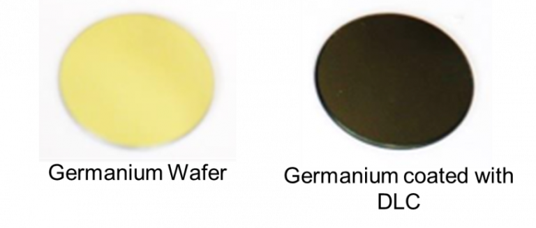
Development of Diamond like Carbon based IR Optics on Germanium
DLC is known to have good IR transmission properties and is currently a favourable choice of IR optics used in harsh environmental conditions. A single layer of DLC coating on either side of a germanium wafer was synthesised and peak transmission was for a wavelength of 2.4 µm was observed to be 96% and for 3-5 µm range, a peak transmission of 96% was observed. The coatings have passed a few tests that were conducted as per MIL-C-48497A standards.This coating has been indigenised for IR transmission. This has been funded by Department of Science and Technology.
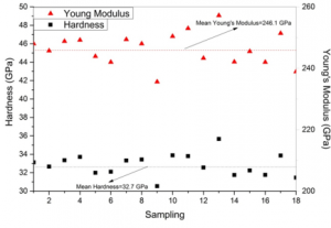
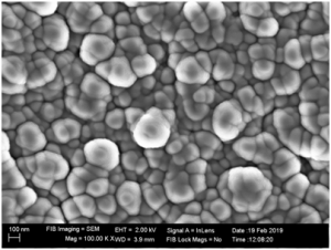
Development of High Hardness Diamond Like Carbon thin films at room temperature
A DLC synthesis process was developed at room temperature using a Roth & Rau RF PECVD with hardness of DLC of about 32.7 GPa using an Agilent G200 Nano Indentor. TEM images (from an FEI Titan G2 60-300) indicated an amorphous – crystalline matrix. The films were also characterised using Raman Spectroscopy (Seki Tecnotron) to evaluate sp3 hybridisation.


Implementation of Diamond Like Carbon on various materials like Silicon, Stainless Steel, Carbon Steel, High Speed Steel, Carbide tools, PMMA, Soda Lime Glass, Ti-Al-V alloy and Aluminium alloys.
An investigation into the mechanism of DLC adhesion on various substrates was undertaken. The adhesion of DLC was studied without the use of any buffer layer in most cases by plasma treatment using various gases.

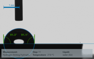
A Veeco Dimension V AFM was used to study to the plasma treated surfaces. This lead to self cleaning surfaces, required on various applications that needs scratch protection and low wettability. A part of this work has been implemented in an Department of Science & Technology project.
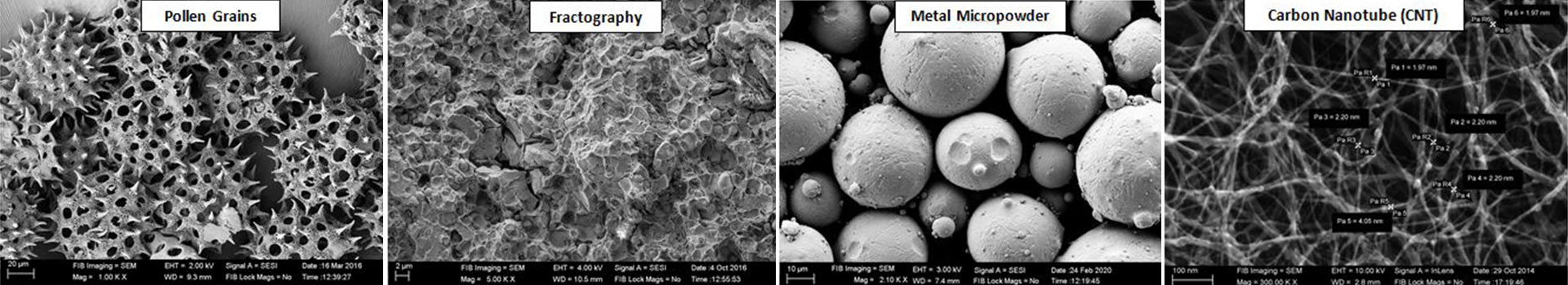
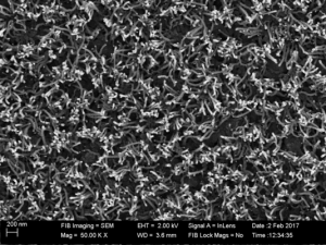
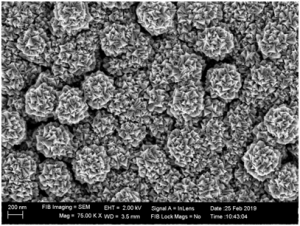
Development of Carbon Nanotubes for super black applications
A feasibility study on synthesis of CNTs on various substrates like Stainless Steel, Silicon, Anodised Aluminium, Anodised Titanium, Titanium was undertaken. Different strategies to achieve a film growth of CNT was employed which included, usage of catalyst layers and optimising the thickness of each of the layer, varying gas ratios of different hydrocarbon gases etc. This is required for components to absorb all light in space. This project was funded by Indian Space Research Organisation.
Proof of Concept Demonstrations
1. Development of UV Sensor head using thin film synthesised carbon nanotubes for monitoring aero engine combustion. The sensor has almost zero hysteresis.

2. Development of thin film micro-heater

3. Development of flexible temperature sensor using thin films on transparent cellulose acetate sheet for aerospace components
4. Development of alternate thin film materials for UV mask plates for MEMS devices.
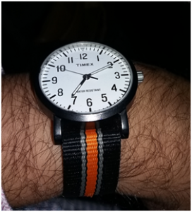
5. Protective thin film coatings for watch casings. Diamond Like Carbon coated on watch case
6. Development of CNT-Ceramic/Metal 2D nanomaterial for mechanical and thermal applications
Laser Processing
Development of Metrology Artefacts:
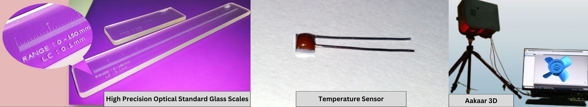
a.High precision optical standard glass scales:

CMTI has developed high precision optical standard glass scales by using state of the art facility available in the Institute. These artefacts are used for the measurement, inspection, calibration and positioning in Imaging Equipments, Microscopy, Scanning etc. The Grating straightness & pitch accuracy of the developed artefacts is within 1 µm.
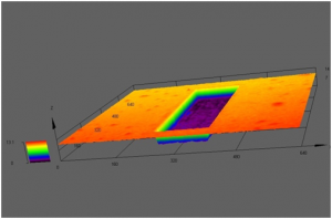
b. High precision optical standard calibration masks:


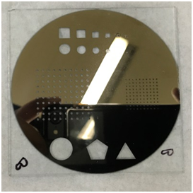
CMTI has developed the high precision optical standard calibration masks for the calibration of Microscopy equipments. A low-reflectivity chrome coating of 100 nm thick was vacuum sputtered on soda lime glass of 1.5 mm thick using in-house physical vapor deposition(PVD) system. Then using KrF- 248 nm laser, the features from 10 µm to 1.5 mm were etched out in the mask without affecting the base substrate.
c. Development of depth master
CMTI has taken an initiative for the indigenous development of metrology artefacts for the Indian industries. We have developed a depth master of width 150 µm and depth of 10 µm in glass using Femtosecond laser micromachining system.
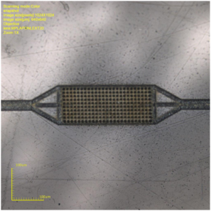
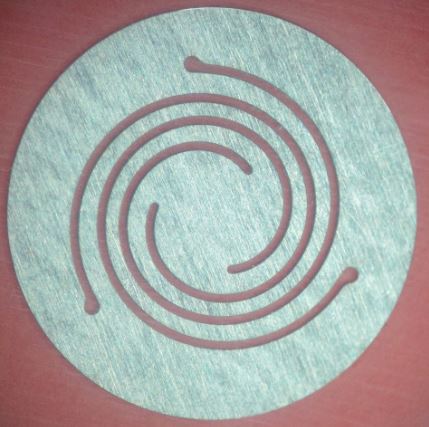
d. Glass gratings for Micro-analyser
By using Femtosecond laser micromachining system four angular gratings were created on glass at four different angles namely 0°, 1°, 3° and 5°. Each grating is having a dimension of 0.2 x 2 mm.
Technology developments in Micro-machining area:
i.Development of technology for marking jewellery Diamonds

Successfully established a process for marking diamonds using ultrafast pulsed laser micromachining system for one of the country’s leading Jewellery maker. The size of the diamond is 1.2 mm where as the marking dimension is 50×100 µm.
ii. Development of Micro-fluidic devices
A microfluidic device was fabricated in glass using femtosecond laser micromachining system having an array of 25×10 of micro holes with Ø 10 µm and depth of 5 µm.
CMTI has also developed a micro-fluidic device for bio-medical application using ultra fast pulsed laser to one of the Indian start-up company. The micro-fluidic channel cross section is around 50 microns and the channel is done on borosilicate glass.

iii. Development of technology for the synthesis of high purity Copper nano particles using ultra fast pulsed laser.
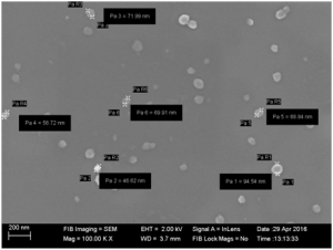
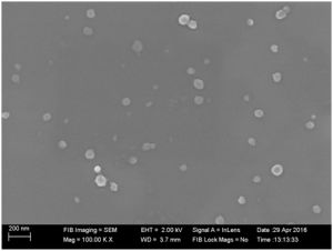
CMTI has successfully established a process to synthesize high purity copper nanoparticles of size 40 – 50 nm.
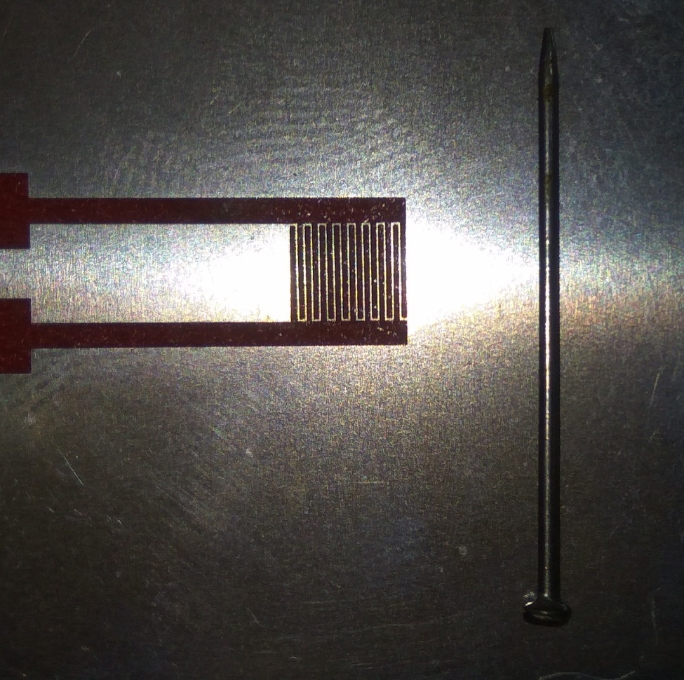
iv.Development of micro-needles for bio-medical applications
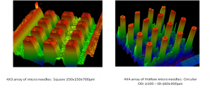
CMTI has developed square and circular micro-needles on Stainless steel and PMMA materials for drug delivery applications.
| Sl. No. | Facility | Industry Charges (Rs) | Academia Charges (Rs) |
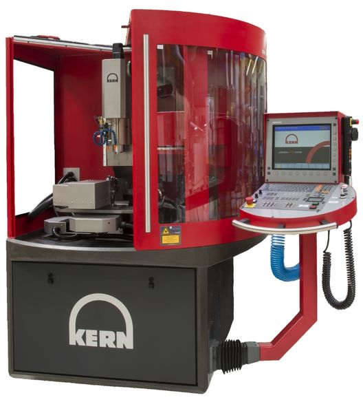
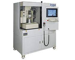
| 01 | Ultra precision 5 Axes Micro Machining Centre – KERN EVO |
2600 | 1800 |
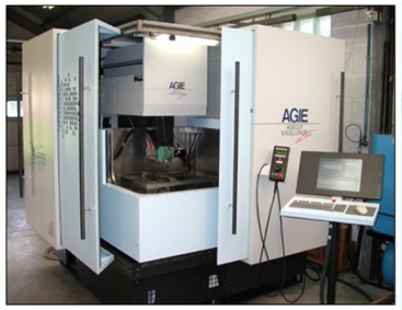
| 02 | Micro Wire Electro Discharge Machine (µ-WEDM) - AGIE EXCELLENCE 2F | 3000 | 2000 |
| 03 | Hard Turn- mill centre - HARDINGE | 2400 | 1600 |
| 04 | Multipurpose µ-EDM Machine – DT 110MICROTOOLS | 2400 | 1600 |
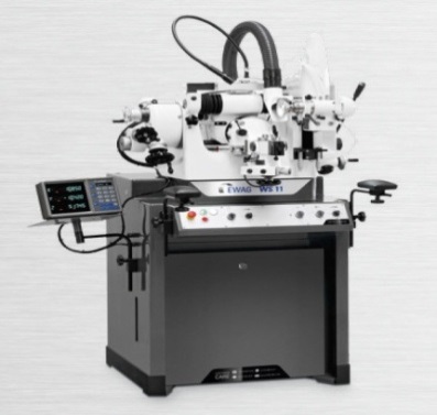
| 05 | Universal Tool and Cutter Grinder Machine - EWAG |
2400 | 1600 |
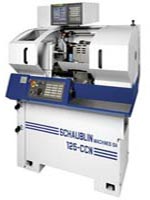
| 06 | Precision CNC Lathe - Schaublin125 CNC |
1000 | 600 |
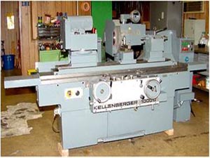
| 07 | Universal cylindrical grinding machine- Kellenberger 1000 U -175 |
1200 | 800 |
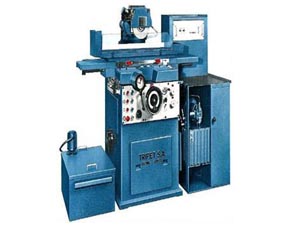
| 08 | Precision Surface grinding machine–Tripet S.A. |
1200 | 800 |
We offer the utilisation of our laboratory services for both deposition using PVD and CVD along with micromachining using lasers. The facilities list consists of all the specifications of the equipment that are available for services.
Specific services include but not limited to the deposition of Diamond Like Carbon, Carbon Nanotubes, Thin film micromachining, Micro fluidic device, sensor micromachining using Excimer and Femto second laser. Please contact us if you have any queries for customised solutions.
| Sl No. | Facility | Charges in Rupees/Hour | |
| Industry | Academia | ||
| 1 | Magnetron Sputtering Physical Vapour Deposition | 4100 | 2600 |
| 2 | Plasma Enhanced Chemical Vapour Deposition | 5900 | 4000 |
| 3 | Femto Second Laser Micromachining | 6100 | 4000 |
| 4 | Excimer Laser Micromachining | 6500 | 4100 |
| 5 | Contact Angle Measurement | 2000 | 1300 |
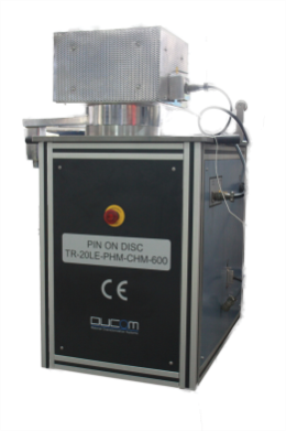
| 6 | Pin On Disk Tribometer | 1800 | 1200 |
*The rates of the services shall be changed periodically. Please contact us for exact prices. Cost of the equipment is based on the usage on a per hourly basis. 18% GST Extra.
The group is equipped with micro machining facilities with state-of-the art equipment/machines for manufacture of components with miniature features and accuracies inthe order of few microns.
- Min Drilling Capability : Ø 30 µm
- Min Milling Capability : Ø 50 µm
- Maximum Spindle speed : 50000 Rpm
- Positional Accuracy : 2 µm
- Manufacturing of micro components.
- Drilling of very small/fine holes.
- Micro channels, micro needles.
- Medical implants, Dental implants.
- Micro dies and micro molds.
- Minimum wire diameter : 30 µm
- Profile Accuracy : 4 µm
- Surface Finish (Ra) : 0.1 µm
- Dies & punchers Micro surgical tools & bio medical devices.
- Thin walled structural parts for Aerospace application.
- Micro channels, Micro dies and molds.
- Machining of Hard Materials up to: 68 HRc
- Maximum turning length : 610 mm
- Maximum Spindle speed : 4200 RPM
- Maximum swing over bed : 519 mm
- Roundness : 0.5µm
- Surface Finish (Ra) : 0.2 µm
- Positional Accuracy : 5 µm
- Machining of hard material upto 68HRc
- Machining of bearing steels
- Machining of hot and cold work tool steels
- Machining of high speed steels
- Machining of die steels

- Working range: X: 200mm, Y: 100, Z: 100mm.
- Spindle speed : 1 – 300 RPM
- Min micro hole drill size : 10 µm
- Micro EDM Sinking min feature size: 50 µm
- Micro shafts & pins
- Micro gears
- Micro filters
- Miniature surgical tools
- Medical implants
- Work head swivel axis, A : -135°/+30°
- Work head inclination axis ,C : ±15°
- In process Measurement capability
- Form tool grinding
- Cutting tools re sharpening
- Customized tools grinding
- Height of centers: 125m
- Maximum distance between centre : 500mm
- Permissible diameter above bed : 270 mm
- Permissible diameter above slide : 130 mm
- Permissible diameter in spindle bore: 28mm
- Permissible diameter in collet B32 :24mm
- Maximum diameter of chuck : 150mm
- Spindle speed ,step less :0-5000 rpm
- Traverse travel,X-axis : 180mm
- Longitudinal travel,Z-axis : 410 mm
- Distance b/w centers:1000mm
- Height of centers:175mm
- Max swing over table:349mm
- Max travel of table:1300mm
- Spindle speed:1500-2200rpm
- Precision cylinder grinding
- Surface grinding
- Internal grinding
- Face grinding
- Tool grinding & execution of special grinding operation
- Maximum slide movement: 530 X 220 mm
- Maximum grinding area : 500 X 200 mm
- Table working surface : 600 X 200 mm
- Variable speed drive : 1150 – 3300 Rpm
- Vertical & Transverse feed movement
- By hand wheel 1 division : 0.01 mm
- By micrometer adjustment : 0.001 mm
- Surface grinding with ultra-precision.
- Form grinding.
CMTI has state of art facilities in thin film deposition and laser micromachining catering to niche applications. The list has been given below. To know more about the facilities please contact us.
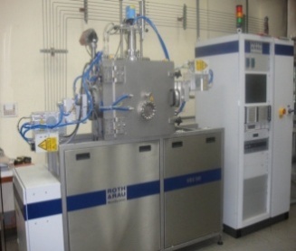
Vacuum chamber Size: 500 × 500 × 500 mm
Coating area: Dia 250 mm
Base Vacuum : 1 × 10⁻⁷ mbar
Plasma source : ECR Microwave & RF
Process Gases : C2H2, CH4,N2, Ar, O2, H2, NH3
Substrate Heater : 700° C
Carbon Nanotubes and Diamond Like Carbon Films
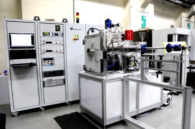
Vacuum chamber Size: D-Type 500 mm
Coating area: 3 x 3” target and 1 x 6” Target with substrate rotation
Target sizes: Maximum 6”
Plasma Sources: RF, DC and Pulsed DC
Base Vacuum : 1 × 10⁻⁷ mbar
Process Gases N2, Ar, O2,
Substrate Heater : 600° C
Metal, Metal Oxide and Metal Nitride Depositions
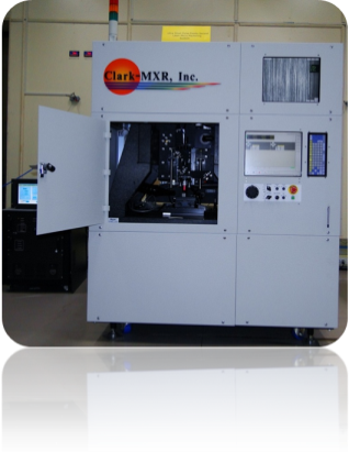
Wave length : 775 nm
Pulse width : 10 ps to 150 fs
Repetition rate : 1 Hz to 2 KHz
Resolution : 1 nm
Minimum feature size : 1 µm
Traverse X, Y & Z Axis : 150 x 150 x 100 mm
Micromachining of Metals, Glasses, Ceramics, Semiconductors & Polymers etc
Wave length : 193 nm (ArF) & 248 nm (KrF)
Pulse duration : 20 ns
Repetition rate : 1-50 Hz
Beam size : 24 x 10 mm
Minimum feature size : 1.5 µm
Traverse X, Y & Z Axis : 200 x 200 x 50 mm
Applications:
Micromachining & Processing of Polymers, Thin Metal Films etc

Effective Drop : 2 µL
Video : 100 fps
Measurement : Only flat samples kept on horizontal table
Temperature : Room
Vacuum : Atmospheric
Contact for Ball and Pin Sizes
Contact Angle Measurement

Disk Dia : 6 inch
Load : 5-100 N
RPM : Upto 1500
Temperature : Room
Vacuum : Atmospheric
Contact for Ball and Pin Sizes
Measurement of Co-efficient of Friction
- Developed technology for precision componentsfor manufacturing with feature sizes in the range of <100 µm with stringent dimensional tolerances in the order of 5-10 µm on metallic and non-metallic parts indigenously. Such components have been regularly supplied to various capital goods and strategic sectors.
List of Relevant Publications
- K. Niranjan Reddy, and K. Chandran, “Development of Ultrasonic Standard Reference blocks of Aerospace Quality”, presented at QUEST-2001 conference, VSSC, Trivandrum.
- G. Jayaraman, V.K. Venkateswaran, and K. Niranjan Reddy, “An Analytical Approach for Precise Positioning of Tool in Diamond Turning”, European Society for Precision Engineering & Nanotechnology - euspen 2001 conference.
- K. Niranjan Reddy, and P.V. Shashi Kumar, “Micro-Drilling of Precision Flat Bottom Holes in Titanium”,presented atCOPEN 2003-04, CMTI, Bangalore.
- K. Niranjan Reddy, P.V. Shashi Kumar, and SomashekarRao, “Micro Finish & Micro EDM Applications in Precision manufacturing”,Manufacturing Technology Today Magazine January 2007 published by NICMAP, CMTI.
- K. Niranjan Reddy, and P.V. Shashi Kumar, “Centering of Tool in Diamond Turning”,presented at 21st AIMTDR, VIT, Vellore.
- V.R. Raju ,M.Chellamalai, P.V.Shashikumar “Study on surface quality and accuracy of hard turned axial feed rollers of honing machine”. - “Int. Journal of Precision Technology” by Inderscience Publishers, Vol. 3, No 1, 2012, 82-90.
- V.R. Raju , Srinivasa C.K ,Vinod A.R, “Study on micro-electrical discharge machining of Steel using copper Electrodes” -1st National Conference on Micro & Nano Fabrication” 2013, CMTI, Bangalore.
- Gopikrishna S, V. R. Raju ,Ankit K, Shashikumar P. V. , “Manufacture of micro sized thread for micro actuator of laser Grating mount”. - Int. Journal of Advanced manufacturing technology” by Springer Publishers, 09 May 2012.
- Karthik M S, Kuppuswamy Ramesh, Raju V.R., Manjunatha M A, Balashanmugam N, “Study on effect of abrasive flow polishing on wear characteristics of ball nose end mill” –COPEN 2019 @ IIT Indore.
- K. Niranjan Reddy*, T. Narendra Reddy, Shashi Kumar, V.R Raju, P.V Shashi Kumar , “Evaluation of Spiral Groove Depth on a Spherical Surface by usingCurve Fitting Algorithm” - International Colloquium on Material, Manufacturing and Metrology, ICMMM 2014 August 8-9, IIT Madras, Chennai, India.
- M.S. Karthik, V.R. Raju., K.Niranjan Reddy, N. Balashanmugam, M.R. Sankar, (2020) “Cutting parameters optimization for surface roughness during dry hard turning of EN 31 bearing steel using CBN Insert.” Materials today: proceedings; DOI:10.1016/j.matpr.2020.02.224
Surface Engineering
Technologies Developed
- Synthesis of Room Temperature Diamond Like Carbon on any surface with high hardness >2500 HV
- MIL – C Standard qualified DLC films for Infra Red Windows for Anti Reflection and Night Vision Application
- Diamond Like Carbon for functional and aesthetic surfaces
- Carbon Nanotube direct deposition on aerospace materials
- Super Black Carbon Nanotubes for space applications
Laser Processing
Technologies & Products Developed
- Development of high precision optical standard glass scales
- High precision optical calibration masks
- Synthesis of high purity copper nano-particles
- Micro-needles for drug delivery applications
- Micro-fluidic channels for Bio-medical applications
Patent filed:
- “System and Method for making micro needles using microstereo lithography”
Indian Patent Office Application No.: 660/CHE/2015 dated 11.2.15
List of Relevant Publications
- AshishVarade, Ankit. K, Niranjan Reddy, M. Chellamalai, N. Balashanmugam, P.V. Shashikumar, “Diamond-like carbon coating made by RF Plasma enhanced chemical vapour deposition for protective antireflective coatings on germanium”, Procedia Material Science, vol. 5, 2014, pp. 1015-1019
- Ankit. K, K. Niranjan Reddy, AshishVarade, M. Chellamalai, N. Balshanmugam, P.V. Shashikumar, “Development of hard DLC coatings at Room Temperature using RF PECVD process”, Presented at International Colloquium on Material, Manufacturing and Metrology, 2014, IIT Madras, Chennai.
- K. Niranjan Reddy, AshishVarade, Ankit. K, J. Joshua, D. Sasen, M. Chellamalai, P.V. Shashikumar, “Double side coating of DLC on silicon by RF-PECVD for AR application”, Procedia Engineering, vol. 97, 2014, pp. 1416-1421.
- AshishVarade, K. Niranjan Reddy, D. Sasen, Ankit. K, M. Chellamalai, P.V. Shashikumar, “Detailed Raman Study of DLC coating on Si (100) made by RF-PECVD”, Procedia Engineering, vol. 97, 2014, pp. 1452-1456.
- Sunil, M, Ankit. K, K. Niranjan Reddy, M. Chellamalai, N. Balashanmugam, “Experimental Investigation of RF Sputtered SiO2 Thin films for evaluation of uniformity” presented at Advances in Metrology, 2016, National Physical Laboratory, New Delhi
- Ankit. K, AshishVarade, SarmisthaDhan, K. Niranjan Reddy, M. Chellamalai, N. Balashanmugam, “Synthesis of high hardness, low COF diamond-like carbon using RF-PECVD at room temperature and evaluating its structure using electron microscopy”, Diamond and Related Materials, vol. 78, 2017, pp. 39-43.
- Ankit. K, AshishVarade, SarmisthaDhan, K. Niranjan Reddy, M. Chellamalai, N. Balashanmugam, “Synthesis of high hardness IR optical coating using diamond-like carbon by PECVD at room temperature”, Diamond and Related Materials, vol.80, 2017, pp. 108-112
- Ankit. K, K. Niranjan Reddy, M. Chellamalai, N. Balashanmugam, “Feasibility of CNT based Sensor for UV Detection in Combustion Process for Aerospace Applications” Proceedings of 10th International Conference on Precision, Meso, Micro and Nano Engineering (COPEN-2017), 2017, IIT Madras, pp. 353-356.
- Ankit. K, K. Niranjan Reddy, AshishVarade, SarmisthaDhan, M. Chellamalai, N. Balashanmugam, “Development of Implementable Diamond-like Carbon Coating for Improving Scratch, Wear and Optical Properties for Practical Industrial Applications”, Proceedings of 10th International Conference on Precision, Meso, Micro and Nano Engineering (COPEN-2017), 2017, IIT Madras, pp. 372-375.
- Ankit.K, Sunil. M, K. Niranjan Reddy, N. Balashanmugam, “Development of Nanometre Edge Resolution Metrology Standards for Video Measuring Systems” Proceedings -Abstract at Advances in Metrology, 2019, National Physical Laboratory, New Delhi
- Sunil. M, Ankit.K, K. Niranjan Reddy, N. Balashanmugam “Process for the Development of high precision gratings/scales” selected at Advances in Metrology, 2019, Proceedings -Abstract at Advances in Metrology, 2019, National Physical Laboratory, New Delhi
- Ankit. K, K. Niranjan Reddy, Gokul, N. Balashanmugam, “Investigation on the effect of nucleation time on CNT growth using RF-PECVD” – Manufacturing Technology Today, Vol. 18 (3), Mar 2019.
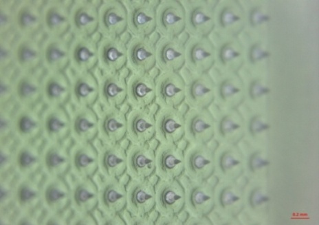
Micro Needles in PMMA and Metals
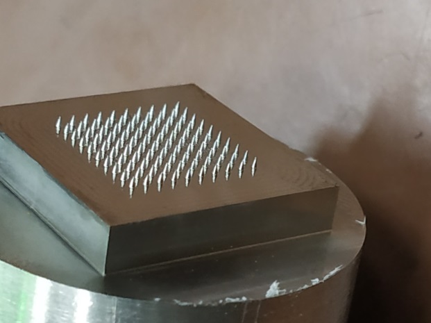
Micro Needles in PMMA and Metals

Precision Micro Components
Precision Micro Components
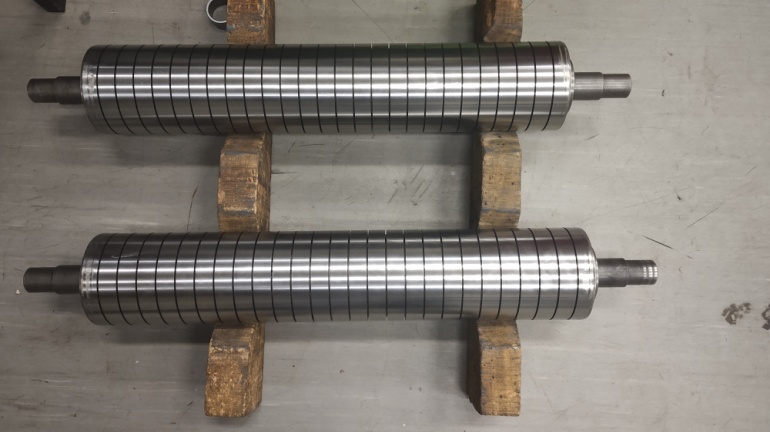
Feed Rollers for Automotive Industries
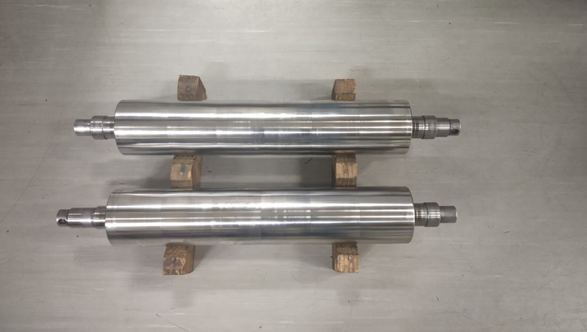
Feed Rollers for Automotive Industries
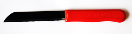
DLC coated Kitchen Knife
Cu Encapsulating CNTs

DLC Coated Guideway

Mask on 200 um thick stainless steel with channel width of 20 um
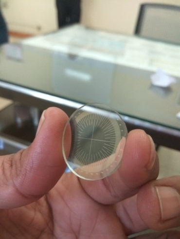
Angular standard glass scale with 1 graduation pitch
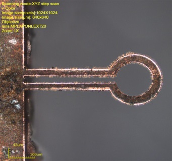
Flexure on 150 um thick spring steel

Flexure on 20 um thick Nickel sheet
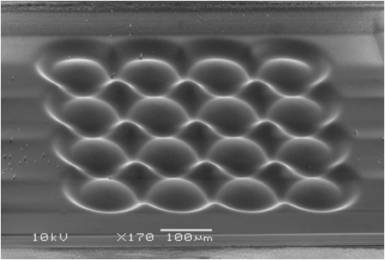
Micro lens array of 100um of PMMA

Micro heater on Tin
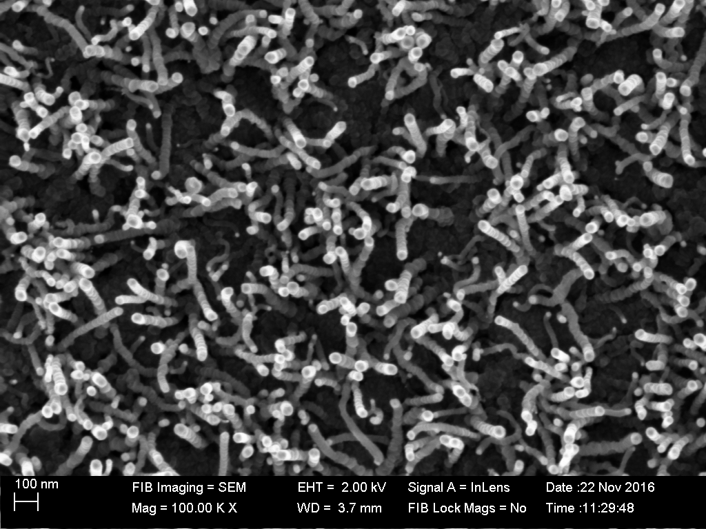
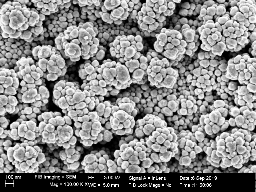
Carbon Nanotubes
Micro cantilever on 5 um thick copper
Technical Queries
Scientist - D
Group Head for Micro-Nano Manufacturing
Centre for Micro-Nano Manufacturing and Metrology (C-MNTM)
Central Manufacturing Technology Institute (CMTI)
Tumkur Road, Bengaluru – 560022
Phone: +91-80-22188391
E-Mail: sunilm[at]cmti[dot]res[dot]in
Scientist - C
Micro-Nano Manufacturing
Centre for Micro-Nano Manufacturing and Metrology (C-MNTM)
Central Manufacturing Technology Institute (CMTI)
Tumkur Road, Bengaluru – 560022
Phone: +91-80-22188383
E-Mail: karthik[at]cmti[dot]res[dot]in
For more details contact
Joint Director & Centre Head (C-MNTM)
Centre for Micro-Nano Manufacturing and Metrology (C-MNTM)
Central Manufacturing Technology Institute (CMTI)
Tumkur Road, Bengaluru – 560022
Phone (Office): +91-80-22188379
Mobile: +91-9449842672
E-mail: niranjan[at]cmti[dot]res[dot]in
Micro-Nano Manufacturing Group
Centre for Micro-Nano Manufacturing and Metrology (C-MNTM)
Central Manufacturing Technology Institute (CMTI)
Tumkur Road, Bengaluru – 560022