- Introduction
- People
- Research Area
- Projects
- Services
- Facilities
- Gallery
- Contact
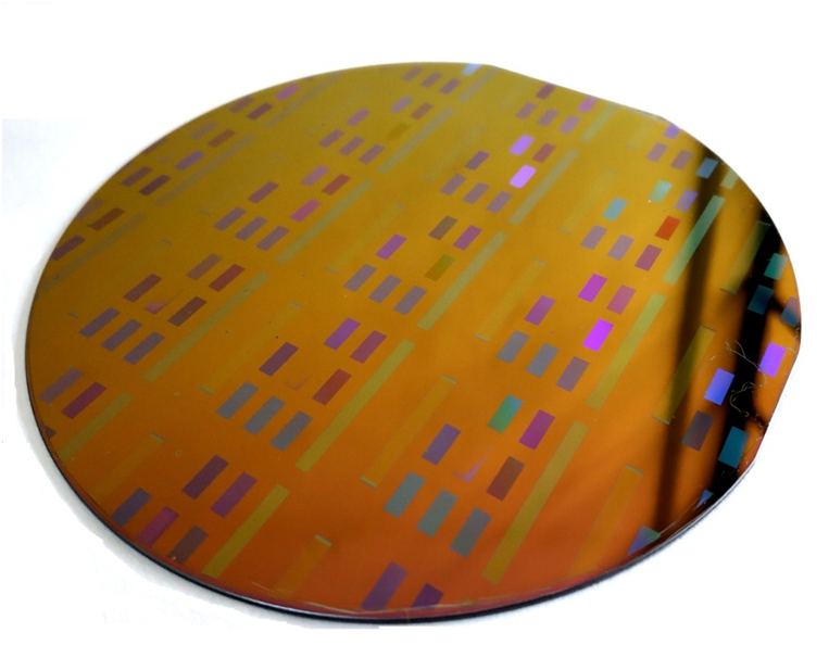
Sensor Technology Development Centre (STDC) is a one
of its kind national laboratory established with 6-inch wafer processing
capability and a dedicated focus on MEMS sensors, microsystems,
electronics, and semiconductor packaging. STDC houses 30+ process tools
catering to the fabrication, characterization, packaging, and validation
of devices and technologies. These process tools are housed inside
state-of-the-art cleanrooms with classifications of ISO-5(Class 100),
ISO-6(Class 1000), and ISO-7(Class 10000) as per the process demand over
a large area of around 1000 sq. meters. This facility is also backed up
with all the necessary utilities at the backend and the much-needed
ground vibration isolation to work at the feature sizes of micrometer
ranges.
The
major objectives of STDC include Research and Development in the field
of indigenous product & process knowledge creation for industry
needs, skilling & human resource development, the proliferation of
sensor-based systems/packages/solutions, support & service as a
Common Engineering Facility Centre for Capital Goods networking with
national & international industry/academia.
STDC
majorly focuses on activities viz., research and development of
innovative and new products such as sensors for machine tools,
automotive, space, aerospace, agriculture, biomedical, healthcare, etc.,
The centre also focuses on the development of technologies in
electronics, and semiconductor packaging such as dicing, bonding, thin
films, electroplating, sealing, wafer level packaging, 3D integration,
System in Package, etc.,
| Centre Head | |||
| Photo | Name | Designation | View Profile |
|---|---|---|---|

|
Mrs. Kusuma N | Scientist - F | View Profile |
| Group Head | |||
| Photo | Name | Designation | View Profile |
|---|---|---|---|
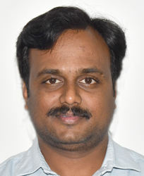
|
Mr. Harsha S | Scientist - D | View Profile |
| Scientists | |||
| Photo | Name | Designation | View Profile |
|---|---|---|---|

|
Mr. Harsha S | Scientist - D | View Profile |
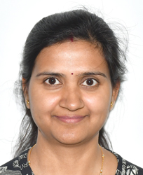
|
Mrs. Megha Agrawal | Scientist - D | View Profile |

|
Mr. Pradyumna J | Scientist - C | View Profile |
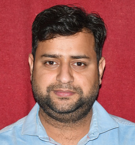
|
Dr. AJAY JASWAL | Scientist - B | View Profile |

|
Dr. Prabhanjan Kulkarni | Scientist - C | View Profile |
| Technical Staff | |||
| Photo | Name | Designation | Phone (Office) |
|---|---|---|---|
|
Mr. Prakash Devadiga | Senior Technical Assistant - I | 080-22188328 |
|
Mrs. Mahalakshmi S | Senior Technical Assistant - I | 080-22188216 |
| Administration | |||
| Photo | Name | Designation | Phone (Office) |
|---|---|---|---|
| Sorry, No Staff are Matched Your Criteria. | |||
- Will be updated with appropriate information shortly
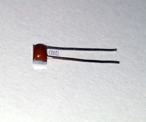
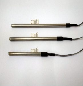
- Design and Development of Thin film based Temperature Sensor for Industrial and Defence applications
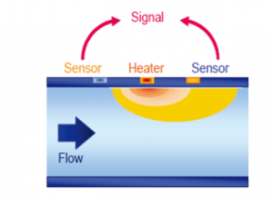
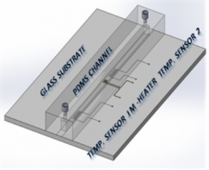
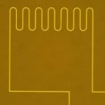
- Thermal based Micro-flow Sensor for drug delivery application

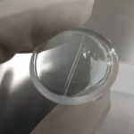
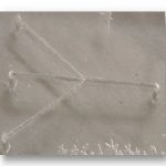
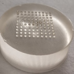
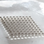
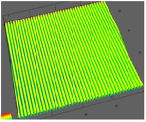
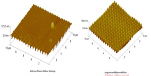
- Polymer device Development using Nano Imprint Lithography (NIL) process: Nano-gratings, Micro-needle array and micro-lens array , Micro fluidic channels, Micro Pillars
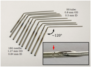
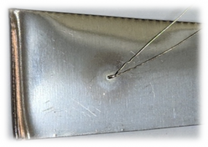
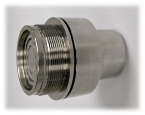
- Electron beam welding (EBW) Process Development
- Advanced packaging of RF MEMS switch: Carrier wafer Fabrication for RF switches using gold electroplating and photo-lithography
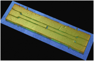
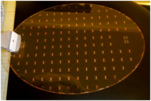
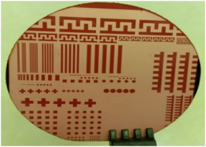
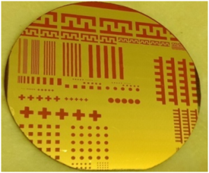
- Thermo-compression wafer bonding for advanced micro-system packaging:
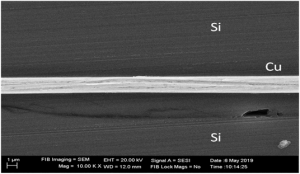
- Silver wire bonding for micro-system Packaging.
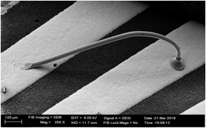
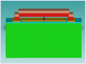

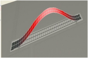
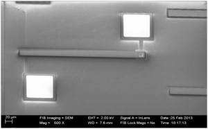
- Technology establishment for Flip chip bonding
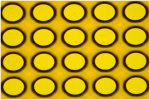
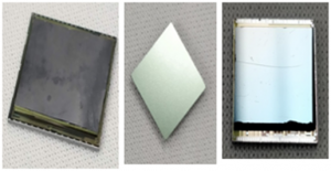
- MEMS design and Analysis
- Silicon and Polymer based Micro device / MEMs fabrication
- Signal conditioning circuit design for MEMS
- Characterization and Packaging of Micro-systems
- Inspection and testing of Packaged Micro-devices
- Internship and M.Tech Projects
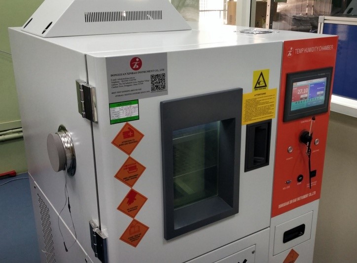
- Temperature Range: -40 to 1850C
- Humidity Range: 10 to 95% Rh
- Chamber Volume: 50 Lts
- Sample Load Capacity: 20 Kg
- Access Port: 4 inch opening with Silicone cork
- Temperature Range: -40 to 1850C
- Humidity Range: 10 to 95% Rh
- Chamber Volume: 50 Lts
- Sample Load Capacity: 20 Kg
- Access Port: 4 inch opening with Silicone cork
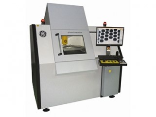
- Geometric Magnification = 2000x
- Can be detect down to 500nm
- Non destructive test of MEMS Packages
- Inspection of defects in Dies, Wafers
- Inspection of PCB defects and casting parts
- Smallest detectable leak rate of 5 x 10-12 mbar l/s.
- Automatic calibration of leak detector with standard fine leak (NIST certified)
- Fine leak inspection of hermetic sealing and qualification of seal.
- Bombing and vacuum inspection of sealed device, to qualify for MIL-STD-883 method 1014 for military and aero space applications.
- Sniffer inspection for fine leak detection

- Pull, push (10 kgf) and shear tests (100 kgf)
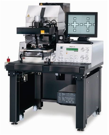
- Supports 80x magnification and fine pitch analysis
- Mechanical characterization of die attach process
- Mechanical characterization of wire bonding process

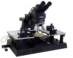
- 6” wafer inspection
- High resolution Micromanipulators – XYZ resolutions ≥ 80TPI
- Electrical inspection of 6” wafer – KGD and quality inspection
- Failure analysis of devices
- Probing of I/O pads on devices from Front End Of Line (FEOL) and Mid End Of Line (MEOL)
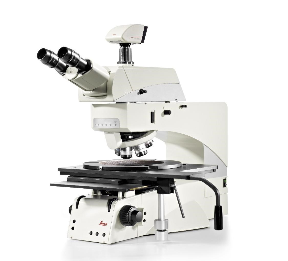
- Various reflected light options like Bright field, dark field, Polarization, Differential Interference Contrast (DIC) and Fluorescence.
- Transmitted light options like bright field and polarization for inspection of transparent specimen like glass and certain polymers
- Inspection, process control and defect analysis in MEMS packaging process
- Structural analysis of materials
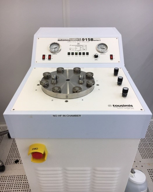
- Liquid CO2 based
- Suitable for wafer sizes upto 6” and small dies.
- Drying of MEMS released structures.
- Drying of high aspect ratio micro structures.Sample preparation for SEM
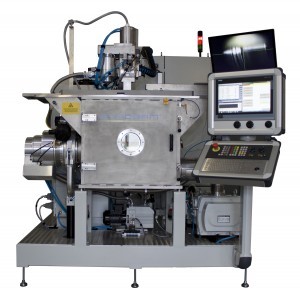
- 6kW, 60kV electron beam gun.
- Twin gun configuration with horizontal gun to avoid sagging of long cylindrical jobs during welding
- Vacuum hermetic sealing of microelectronic components.
- Military and aerospace applications where reliability of the system is important, Hermetic sealed micro electronics is essential.
- Micro joining and macro joining of dissimilar materials
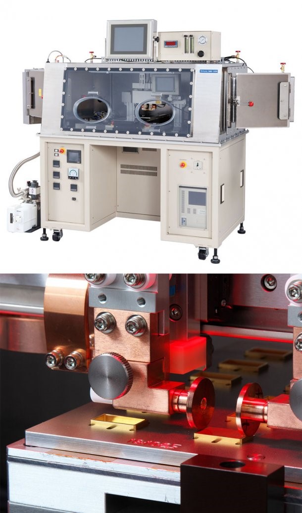
- Resistive welding of different package size ranges from 3mm to 150mm.
- Multiple packages seam sealing in one fixture
- N2 based hermetic seam sealing of micro electronics.
- Military and aerospace applications where reliability of the system is important, Hermetic sealed micro electronics is essential
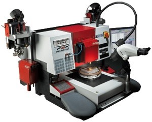
- Semi-automatic wire bonder
- Performs Ball-wedge, wedge-wedge and deep access bonding
- Capable of Copper bonding
- Au, Al, Cu wire bonding for MEMS
- Gold ball bumping
- Copper bonding
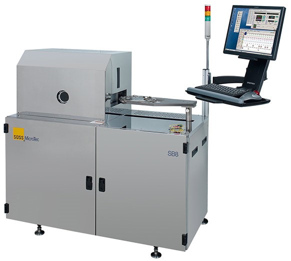
- Wafer bonding of two or more wafers of size
- upto 6” and small dies.
- Suitable for Thermo-compression, Anodic,
- Fusion, Glass frit and Adhesive bonding
- Bonding force: upto 20 kN
- Temperature: upto 500°C with ± 2%
- Uniformity
- Manufacturing of MEMS sensors
- Wafer level Packaging of MEMS sensors
- 3D packaging of MEMS+ASIC
-
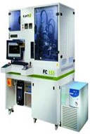
- Thermo compression, reflow, eutectic, epoxy and Thermo sonic bonding capability
- Formic acid vapor tool configuration
- Autocollimator & Advanced Laser leveling system
- Fragile material compatibility
- Temperature up to 450 degree C
- Force range up to 100 kg
- Fine pitch bonding of 15 µm achieved
- Multi chip modules
- Wireless multi stack chip bonding
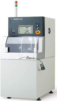
- Sub-merged dicing for released structures
- Can dice 6 inch wafer
- Dicing of released MEMS sensors
- Dicing of wafers and smaller dies
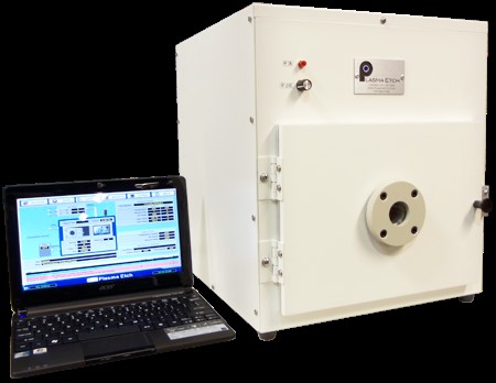
- Programmable process control 0 to 300 W,
- wide range RF power supply
- Surface preparation for wire bonding and die attach process
- Contamination removal in the MEMS packaging process
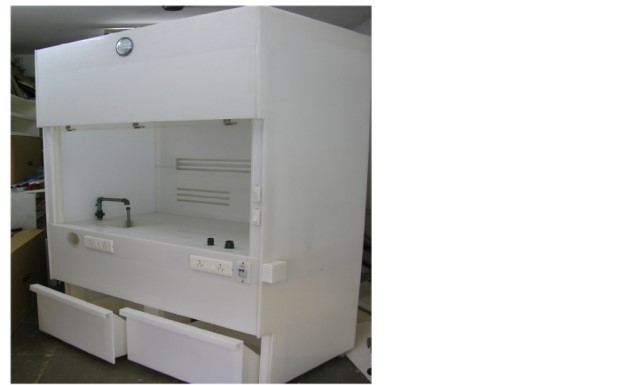
- NPP and SS perforated top with Laminar flow
- Cleaning of Wafers/ die/ samples using different process.
- Etching of different materials.
- Photo-resist coating and its development
- Wafer cleaning and chemical processing
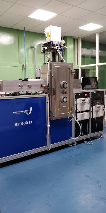
- 10 kW and 6 kW Twin gun configuration for co-evaporation.
- Chamber vacuum of up to 3×10⁻⁷ mbar
- Suitable for single wafer handling up to 6“
- Equipped with a grid less ion source and effusion cell
- Load lock and variable source to substrate distance from 500-700 mm
- Substrate heating up to 600 oC and max 30 rpm substrate rotation
- Intermediate metal layer deposition in 3D packaging
- Optical coatings
- Insulating dielectrics deposition in fabrication and stacking approach
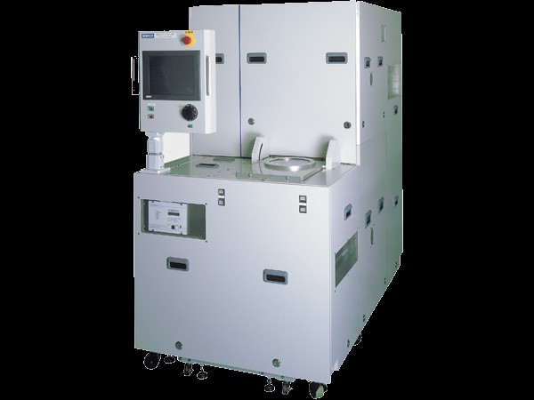
- 6″ Wafer Processing
- Manual Wafer Loading, Automated Robot Transfer To Load-lock Chamber
- ESC With Active Wafer Temperature Control (Helium Backside Cooling)
- High-speed Gas Line System For Improved Response And Smoother Sidewalls
- Notch Prevention Package For SOI Applications
- TSV formation for Advanced Micro-system Packaging
- High Aspect Ratio Micro-structures
- Electroplating Station designed for MEMS/NANO and High density Interconnects.
- Dedicated Cu & Gold Plating Tanks. Suitable
to deposit any metal or alloy from aqueous solution. - Suitable for deposition on small sized dies (20mm X 20mm) and wafers upto 6″ Wafers
- Deposition Uniformity :>5% across the wafer
- Gold, Copper Electroplating for MEMS devices
- Electrodes metallization

- Individually temperature controlled heaters with max 450oC.
- 20 KN force achieved with high degree of uniformity of pressure distribution.
- Pattern size up to 50nm
- Polymer Micro needle array
- Polymer Micro fluidic channel
- Polymer Micro lens array

- Wafer thickness ranging from 0.1 to 10mm can be handled upto to 6″ diameter.
- Can achieve feature size up to 50nm.
- Polymer Micro Optics
- Polymer Micro fluidic channel
- Polymer Micro lens array
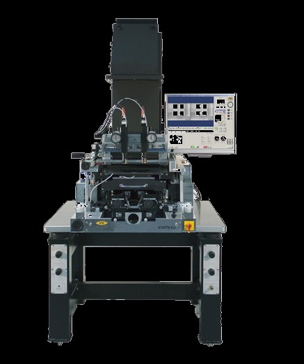
- Wafer handling capacity: upto 6 inch
- Spin coating of Photo resists, Polymers, Anti sticking coatings (ASL), Adhesives, Promoters
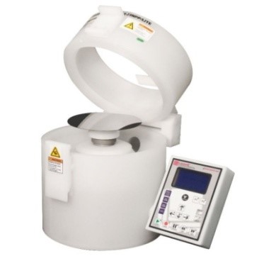
- Handles wafers upto 6 inch
- Alignment accuracy = ± 1µm
- Performs bond alignment
- photolithography for fabrication of MEMS devices
- Master mold creation for Nano Imprint Lithography
Mrs. Kusuma N
Centre for Sensors, Vision Technology and IT
Central Manufacturing Technology Institute (CMTI)
Tumkur Road, Bengaluru - 560 022
Phone (Office): +91-80-22188349
Mobile: +91-9449842664
Fax: +91-80-23370428
Email: kusuma[at]cmti[dot]res[dot]in
Mr. Harsha S
Group Head for Sensor Technology Development Centre(STDC)
Central Manufacturing Technology Institute (CMTI)
Tumkur Road, Bengaluru - 560 022
Phone (Office): +91-80-22188323
Mobile:+91- 9449842665 / 9008420744
Fax: +91-80-23370428
Email: harsha[at]cmti[dot]res[dot]in


